
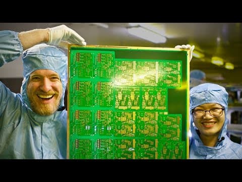
This blog post explores the intricate manufacturing process of printed circuit boards (PCBs) at the JLCPCB factory in Huizhou, China, detailing each step from design file submission to final testing and shipping.
Printed circuit boards (PCBs) are essential components found in nearly every electronic device we use today. Despite their complex appearance, the manufacturing process of PCBs is quite systematic and organized. In this blog post, we will take a detailed look at how PCBs are made, based on a factory tour at JLCPCB in Huizhou, China.
PCBs consist of tiny copper wires sandwiched between layers of fiberglass. These wires connect various integrated circuits and electronic components, forming an organized electronic circuit. The manufacturing process involves several critical steps, starting from the design phase to the final product ready for shipment.
The journey begins at the JLCPCB headquarters in Shenzhen, where engineers review design files submitted by customers. This step is crucial as it ensures that the design is manufacturable. Engineers check for missing layers, borders, and drilling files to confirm that the design meets the necessary specifications.
Once the design is approved, the next step involves printing the design onto a clear film. This film will later be used to project the image onto a copper circuit board blank that has been coated with photoresist material. The preparation of the blank is essential, as it sets the stage for the subsequent steps.
The raw material for PCBs is typically FR-4 fiberglass, which has copper layers on both sides. The large sheets of this material are cut down to size, and the edges are smoothed to ensure a clean finish. This preparation is vital for the integrity of the final product.
In a clean room environment, the inner layers of the PCB are created. A plastic dry film is applied to both sides of the board, which will harden when exposed to UV light. The areas not exposed to light will wash off, protecting the copper during the etching process that follows.
After exposure, the boards undergo a developing process where excess photoresist is washed away. The boards are then placed in an alkaline solution that chemically removes unwanted copper, leaving behind the desired circuit pattern. This step is crucial as it defines the electrical pathways on the PCB.
Once the etching is complete, the inner layers are inspected using Automatic Optical Inspection (AOI) technology. This process ensures that the etched patterns match the original design files, maintaining quality control before moving on to the next steps.
The next phase involves sandwiching the inner layer between copper layers and prepreg (a fiberglass material soaked in epoxy). This assembly is then subjected to heat and pressure, which melts the epoxy and binds the layers together, resulting in a laminated PCB.
After lamination, the boards are drilled to create holes for components. Different types of holes are drilled, including vias, which connect different layers of the PCB. The drilling machines are highly automated, allowing for precision and efficiency.
Following drilling, the boards undergo a copper plating process. This step involves plating copper inside the drilled holes to ensure electrical connectivity between layers. The process is critical for the functionality of multi-layer PCBs.
Next, a solder mask is applied to the outer layers of the PCB. This mask, typically green, protects the copper traces and prevents solder from bridging between pads during assembly. The application process involves both manual and automated methods to ensure even coverage.
After the solder mask is applied, silkscreen printing is used to add markings and labels to the PCB. This step is essential for identifying components and ensuring proper assembly. Different methods are used depending on the quantity of boards being produced.
The final surface treatment enhances the solderability of the copper pads. One common method is Hot Air Surface Leveling (HASL), where the boards are dipped in liquid solder and then blown dry with hot air, resulting in a smooth, solder-ready surface.
Once the boards are fully processed, they are cut into individual PCBs. Each board undergoes rigorous testing to check for electrical connectivity and ensure that all connections are correct. This testing phase is crucial to prevent defects in the final product.
Finally, the completed and tested PCBs are packaged and labeled for shipment. The entire process, from design submission to shipping, can take as little as 24 hours, showcasing the efficiency of modern PCB manufacturing.
The manufacturing of printed circuit boards is a complex yet fascinating process that involves numerous steps and meticulous attention to detail. The tour of the JLCPCB factory highlighted the advanced technology and skilled labor that go into producing these essential components of modern electronics. Understanding this process not only sheds light on the intricacies of PCB production but also emphasizes the importance of quality control in the electronics industry.