
This blog post explores the history, manufacturing process, and significance of printed circuit boards (PCBs) in modern electronics, detailing their evolution from manual connections to sophisticated designs.
Printed circuit boards (PCBs) are essential components in virtually all modern electronic devices. This article delves into what a PCB is, its historical development, and the intricate manufacturing process that transforms a simple copper sheet into a sophisticated electronic device.
Before the invention of PCBs, electronic components were manually connected using wires in a point-to-point construction. This method was not only prone to errors but also made scaling production difficult. Additionally, repairing damaged circuits was a tedious and unreliable task.
In 1936, Paul Eisler, an innovative engineer working for a newspaper company, recognized these challenges and invented the concept of printing conducting copper circuits on a non-conductive board. This groundbreaking idea led to the creation of the first PCB, which laid the foundation for modern electronic design.
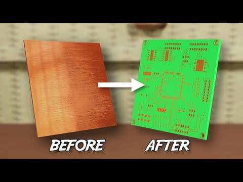
Today’s PCBs are far more sophisticated than their early counterparts. The manufacturing process begins with a simple copper flat sheet, which undergoes several steps to evolve into a complex electronic device.
The process starts with laminating a layer of copper foil onto a flat sheet of insulating glass fiber material. This glass fiber provides mechanical support to the PCB and remains throughout the manufacturing process. The assembly is then sent for drilling, where registration holes are created. These holes serve as reference points for alignment in subsequent steps.
An engineer designs the circuit using computer-aided design (CAD) software. This software generates design files known as Gerber files, which contain detailed 3D models of the PCB. Using these files, a drilling machine creates various holes for component attachment.
After drilling, the boards are thoroughly cleaned to remove any residue. The next crucial step is the production of tiny copper traces through a chemical process called etching. A resistive mask, patterned according to the circuit design, is applied to the copper plate. When the assembly is dipped into an alkaline solution at temperatures between 60 to 120 degrees Celsius, the uncovered copper dissolves, leaving behind the desired traces.
Once the etching is complete, the protective mask is washed off, revealing the copper traces. The quality of these traces is inspected using an optical inspection machine, which compares the printed boards against the design files. Any boards with broken or short-circuited traces are rejected.
Have you ever noticed that PCBs are typically green? This color comes from a layer of solder mask resin applied to protect the board from oxidation and dust. The solder mask is insulating, preventing connections between copper traces and component edges. To ensure proper adhesion, a chemically resistant mask is applied to the edges of the holes before the UV process is conducted to remove the solder mask from those areas.
The final step involves printing a silk screen layer, which includes markings, logos, and symbols to identify PCB components. At this point, the PCB is ready for dispatch to industries.
Once the PCB reaches its destination, components are placed and soldered using liquid tin, affixing them to the copper pads on the board. The final flying probe testing checks the connectivity between all components, traces, and pads to ensure functionality.
The PCB technology discussed here is known as Through-Hole Technology (THT), which, while educational, is becoming obsolete. The latest advancements in PCB technology are based on Surface Mount Technology (SMT), which will be explored in future discussions. Understanding the manufacturing process of PCBs highlights their critical role in the functionality of modern electronic devices, making them the backbone of contemporary technology.